Using airhdl to Design a PN Sequence Checker for Analog Devices ADCs

Analog Devices Analog-to-Digital Converters like the 14-bit AD9645 feature built-in pseudo-random sequence generators, which are invaluable when it comes to checking that the ADC samples can be transmitted error-free to a receiving device, such as an FPGA, over a high-speed link. When bringing up a board featuring such an ADC-to-FPGA link, you want the ADC to output a known pattern so that you can check that the FPGA is indeed receiving the expected data.

For initial smoke tests, a fixed or a checkerboard pattern is fine, but in order to thoroughly check that your data transmission is working error-free, you will want to use more “difficult” test patterns like the PN9 and PN23 ones. Those are industry-standard sequences, which can easily be generated (and checked) using circuits called linear-feedback shift registers (LFSRs). In case you’re not familiar with them, LFSRs are just a chains of registers, with a few strategically placed XOR-type feedback taps.

The difference between the PN9 and the PN23 patterns is the sequence length. The PN9 sequence repeats every 2^9 – 1 = 511 cycles, whereas the PN23 sequence repeats every 2^23 – 1 = 8388607 cycles. This makes the PN23 sequence more suited for higher data rates, as the bit patterns repeat less often than with the PN9 sequence. Also, the PN23 will have longer sequences of contiguous zeros and ones than the PN9 sequence, which is of importance for AC-coupled links. In general, the PN23 sequence is considered more difficult than the PN9 sequence.

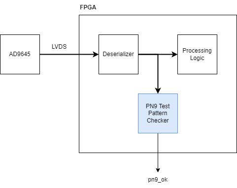
To bring up a board like the one shown below, with an AD9645 outputting samples over an LVDS link and an FPGA receiving them, I like to have the test pattern checker(s) built directly into the FPGA. In this article, I’ll show you how to implement such a test pattern checker using the LFSR components generated by the web-based airhdl code generator. We’ll be looking at the PN9 checker, but once you understand how it’s done, you’ll find it very easy to design your own checker for PN23 or other sequences.

Built-in test pattern checkers are great for board bring-ups.

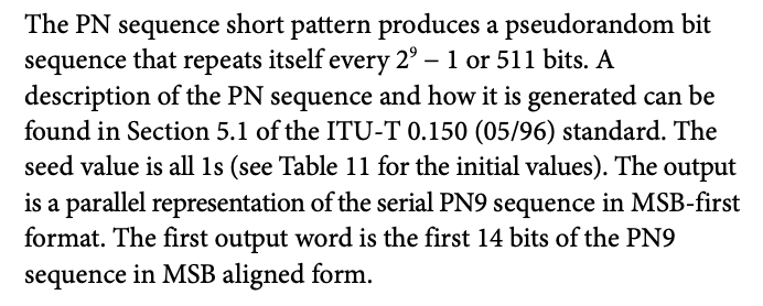
First let’s look at the AD9645 datasheet to find out how to PN9 sequence (also called the PN sequence short) is defined:

PN sequence short description (source: AD9645 datasheet)

The description above is only part of the information we need to fully define the PN9 sequence. The missing part is the generator polynomial, which is given in another part of the datasheet as X^9 +X^5 +1. This is very mathematical way of describing a 9-bit shift-register with XOR feedback taps at bit positions 9 and 5 (using 1-based bit indexing).

The datasheet also gives the first words of the PN9 and PN23 sequences, which is super valuable information because it will allow us to easily check that we’re indeed generating the correct sequence:

The first words of the AD9645 PN sequences (source: AD9645 datasheet)

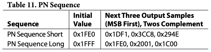
To create a PN9 checker, we’ll be generating the expected PN9 sequence internally in the FPGA and checking that the words we receive from the FPGA actually match the expected ones. Of course, we’ll need to somehow synchronize the internally-generated sequence with the received one. For that, we’ll just wait until the initial value shown in the table above (0x1FE0) is received and then we’ll let our internal sequence generator update on every received word.

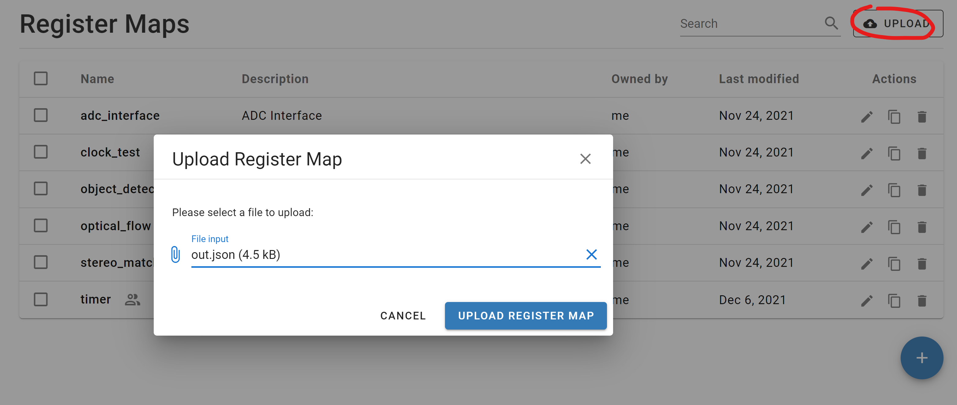
The first step is to head over to airhdl.com. After you have logged in, select the LFSRs entry in the left sidebar to show the Linear-Feedback Shift Registers view, and click the round “+” action button to bring up the New LFSR dialog:

The airhdl New LFSR dialog

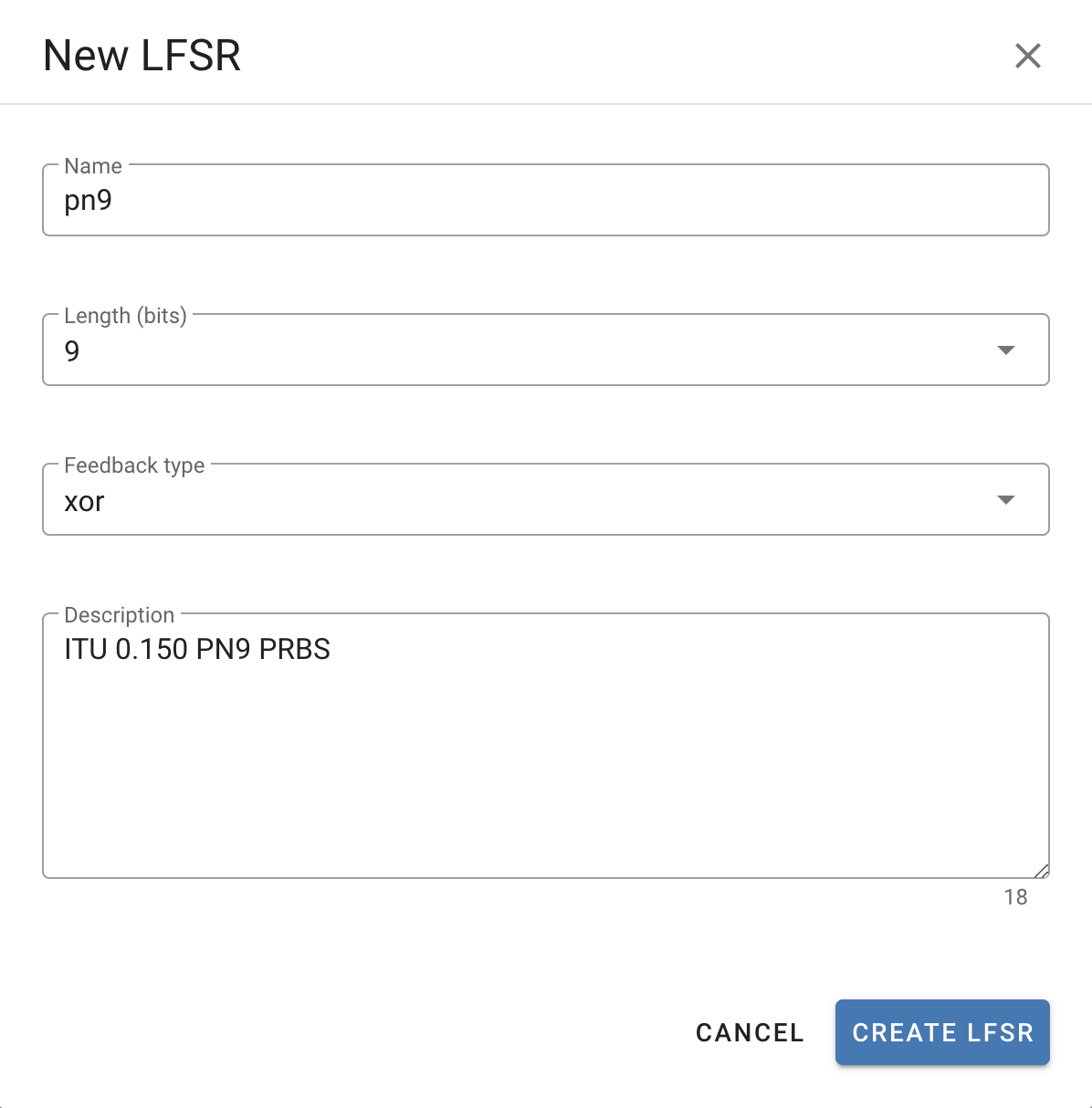
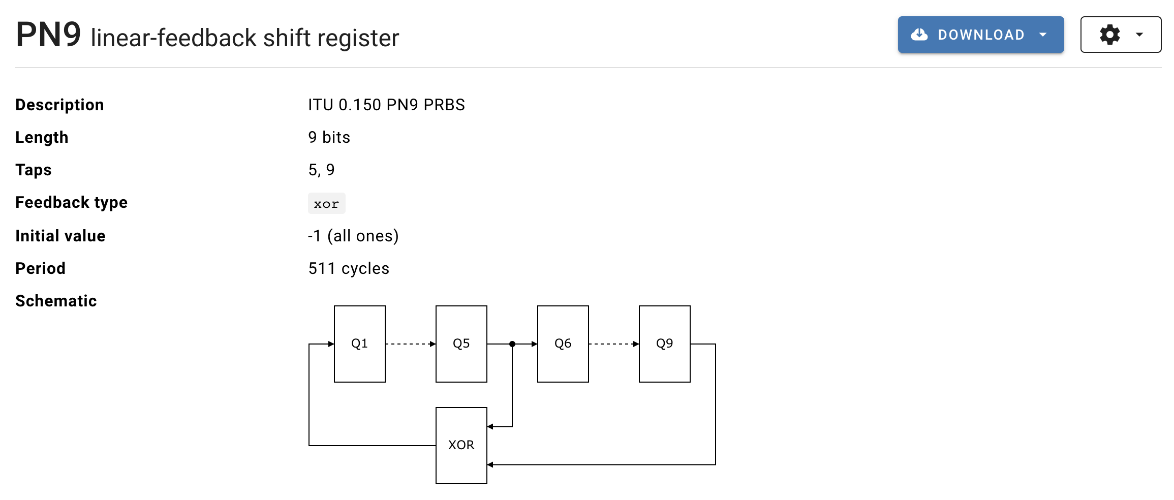
By setting the length to 9 bits and the feedback type to xor, airhdl will generate the following LFSR circuit. Note that based on the configured length of the LFSR (9 bits), airhdl automatically computes the correct positions of the feedback taps (5 and 9):

The generated 9-bit LFSR circuit

If you’re curious about the sequence of numbers that the circuit shown above generates, you can download the corresponding Python model and run it like this:

% python PN9_lfsr.py
1FF
1FE
1FC
1F8
1F0
1E0
1C1
183
107
00F
01E
03D
07B
0F7
1EF
1DF

The output above shows the first 16 states of this 9-bit LFSR (as we have said above, the sequence repeats every 2^9 – 1 = 511 cycles). This is not exactly the sequence that the AD9645 will output when placed in the PN9 test mode though, as the AD9645 is a 14-bit ADC and the PN9 circuit has a 9-bit word length. The AD9645 datasheet explains how to construct the 14-bit words from the LFSR output:

Source: AD9645 datasheet

Using the airhdl-generated Python model for our PN9 LFSR, let’s look at the first 14 output words in binary form (we can use the -r bin option for that):

% python PN9_lfsr.py -r bin 14
111111111
111111110
111111100
111111000
111110000
111100000
111000001
110000011
100000111
000001111
000011110
000111101
001111011
011110111

As explained above, we can construct the first 14-bit word of the PN9 sequence by concatenating the MSBs of the LFSR’s first 14 output words: 11_1111_1110_0000. In order to match the two’s complement sequence that is indicated in the datasheet, we also need to invert the MSB, which gives us 01_1111_1110_0000 = 0x1FE0. This nicely matches the initial value of the PN sequence short from the table above!

Of course, there is always the risk that this is pure coincidence and a bit of paranoia is always a good thing for a developer; so let’s compute one more output word. This time we’ll ask our Python model to output the first 28 LFSR output words, and take the MSBs of the last 14 words:

% python PN9_lfsr.py -r bin 28  
(...)
111101111
111011111
110111110
101111100
011111000
111110001
111100010
111000101
110001011
100010111
000101110
001011100
010111001
101110011

The corresponding output word, again obtained by concatenating the MSBs of the 9-bit LFSR states equals 11_1101_1111_0001. Inverting the MSB and converting the word to hexadecimal gives 0x1DF1, which matches the second output sample of the PN sequence short in the table above. At this point, the result being a pure coincidence is quite unlikely and we’ll assume that our algorithm works fine.

We now have a clear understanding of the algorithm for generating the 14-bit PN9 sequence. The next step is to design the corresponding checker circuit, using a hardware description language such as VHDL. As a starting point, we can download the VHDL package for our pn9 LFSR from the airhdl.com website. This package contains all the constants and a function we need to get us started:

The VHDL LFSR package generated by airhdl.com

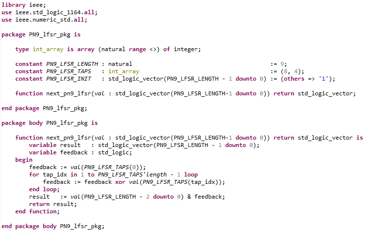
In particular, the next_pn9_lfsr function allows us to compute the next LFSR state, given the current one.

The principle of operation for our checker is as follows:

  1. Receive the first 14-bit ADC output word, let’s call it adc_output[n].
  2. Using the next_pn9_lfsr function, compute the next expected ADC output word; let’s call it adc_expected[n+1].
  3. Wait for the next ADC output word, adc_output[n+1], and compare it to adc_expected[n+1]. If both values match, declare the test pattern checker synchronized and proceed with step 2. If there is a mismatch, the pattern checker is not synchronized and re-start at step 1.

The checker has two states: SYNC and TRACK. In the SYNC state, the checker waits until the PN9 initial value, which is given in the datasheet as 0x1FE0, appears on the data input. When that happens, the checker jumps into the TRACK state where it checks that every subsequent input word matches the next expected word from the PN9 sequence. As long as this is the case, the checker is considered synchronized and this is reflected by the pn9_ok output port being asserted high. If at any time an input word doesn’t match the next expected word, the checker immediately de-asserts its pn9_ok and jumps back into the SYNC state.

When doing hardware tests, you can connect the pn9_ok signal to a debug port of your FPGA design for easy monitoring using an oscilloscope. That way you can just trigger on falling edges of the pn9_ok signal to catch any bit errors, even transient ones.

The VHDL code for the PN9 checker, including a VUnit testbench, is available on the airhdl GitHub. We hope you’ll find this useful!

How to Import 100 Registers from a Text File to airhdl

One of our users recently asked how he could import a list of 100 registers into airhdl without having to create every single register by hand in the user interface. He had the names of the registers available in a text file, one name per line:

REG_0
REG_1
REG_2

REG_99

Subscribers to the airhdl Professional CL plan can import register maps into airhdl by uploading a JSON file whose structure is described in the documentation.

To help import the user’s registers into airhdl, we have created a small Python script that transforms the user’s text file into an airhdl register map JSON object. The script, which is called regs2json.py, is available on our GitHub page. It can be used as follows:

python regs2user.py registers.txt map_name

Where registers.txt is the path to the text file containing the register names and map_name is the name of the register map to be created. The script generates an output file called out.json in the current working directory, which looks like this:

{
  "jsonVersion": 2,
  "registerMap": {
    "name": "my_map",
    "description": "",
    "width": 32,
    "baseAddress": 0,
    "addrWidthBits": 32,
    "revision": 1,
    "generateRecordPorts": false,
    "registers": [
      {
        "type": "Register",
        "name": "REG_0",
        "description": "",
        "access": "READ_WRITE",
        "addressOffset": 0,
        "size": 32,
        "fields": [
          {
            "name": "value",
            "description": "",
            "bitWidth": 32,
            "bitOffset": 0,
            "reset": 0,
            "selfClear": false
          }
        ]
      },
      ...
    ]
  }
}

The last step is to upload the generated out.json file to the airhdl web application using the Upload button in the Register Maps view:

This creates a new register map with the name that we have specified when executing the regs2json.py script (in this example, my_map):

The out.json file can also be used as an input to the airhdl command line generator, which can generate all the airhdl output products (VHDL and SystemVerilog RTL code, testbenches, C header and documentation) locally on the user’s machine:

java -jar airhdl-cl.jar out.json

As we have seen, all it takes is a few lines of Python code to turn a text file into an airhdl register map JSON object that can be either uploaded to the airhdl web application to create a new register map, or used locally as an input to the airhdl command line generator.

How to initialize 30,000 coefficients over AXI4 using airhdl (and a bit of custom logic)

One of our airhdl users recently asked how he could use an airhdl-generated register bank to initialize the 30,000 (or so) weights of a neural network circuit.

When dealing with such large numbers of coefficients, it’s not practical to create a dedicated addressable register for every coefficient as the corresponding logic becomes too large and and slow. What you can do instead is to either store them in a memory, which is very efficient in terms of logic resources, or in a register chain in case you need to concurrent access to the coefficients.

The memory option is quite straightforward as airhdl allows you to create memory-typed register map elements, which you can connect to a block memory components as shown in this article. The downside of this option is that you can only access one element at a time from the user logic.

In the register chain option, the coefficients are stored in the flip-flops of a large shift register, which gives you concurrent access to all of the elements. To implement the register chain, you will first need to create a write-only register (e.g. weight) with a value field corresponding to the width of your coefficients (e.g. 10 bits):

Consequently, the following user output ports are exposed in the generated RTL component:

weight_strobepulsed every time a new value is written to the weight register
weight_valuethe current value of the weight.value register field

You then connect those ports to the input of a 30,000-deep shift register that is part of the user logic, with the weight_strobe acting as a clock-enable to the shift register. To initialize the shift register and thus your coefficients, all you have to do is write the 30,000 coefficients in a row over the AXI4 interface to the weight register using a fixed address pattern. Make sure not to use an incrementing address pattern as there is really only one adressable register in the register bank.

One issue you may run into while implementing this circuit is the high fanout on the weight_strobe signal, which can cause excessive delays and thus timing violations. Here are two ideas to improve the situation:

  • Split the register chain into several smaller chain, each connected to a dedicated register.
  • Route the weight_strobe net through a global buffer like a Xilinx BUFG or BUFR. This adds a fixed delay to the net but in exchange the signal can then be distributed with low skew to a large number of cells.

We hope you will find this useful. To stay informed about what’s going on at airhdl, please follow us on twitter or on LinkedIn.

How To Integrate an airhdl Register File in Xilinx Vivado 2015.3

AirHDL is a free, web-based EDA tool for managing Xilinx ZYNQ and MicroBlaze register files. In this post, I will show you how to integrate an AirHDL-generated register file in a Xilinx ZYNQ design using Vivado 2015.3.

For the purpose of this article, I will use the “Base Zynq” example project that comes with Vivado. It’s a block diagram design of a simple Zynq processsing system with two peripherals: a GPIO and a block memory.

2016-01-18_10-37-14

What we’re going to do is add a custom bus peripheral component with an AirHDL-generated register file to this design.

In Vivado, open the “Address Editor” view and look for a free address range for the register map that you’ll create in AirHDL.

2016-01-18_10-42-51

I will use 0x4200_0000.

In AirHDL, create a new register map called “myMap” and make sure to use the base address you selected before (in my case: 0x4200_0000) as the regitster map’s base address:

2015-12-26_17-44-47

Add a few registers to the newly created register map. I will add a read-write “control” register with a 1-bit “value” field and a read-only “status” register with also a 1-bit “value” field. In AirHDL, each register field will map to a separate port in the generated RTL component.2015-12-26_17-48-38For every register map that you create, AirHDL generates a number of different output products that you can download:

  • C Header
  • VHDL Package
  • VHDL Component
  • VHDL Instantiation Template
  • VHDL Testbench
  • HTML Documentation
  • IP-XACT Specification
  • JSON Specification

For the purpose of the integration into a Xilinx Vivado hardware design, the only files that you need are the VHDL Package and the VHDL Component. Download these and save them into an empty folder on your hard drive (e.g. e:\temp\mymap).

2015-12-26_18-06-50

Back in Vivado, select Tools > Create and Package IP…

Select “Package a specified directory” and select the directory containing the downloaded AirHDL files (in my case: e:\temp\mymap).

2016-01-18_10-44-58

In the automatically created IP project, check that the ports and interfaces are correct. In particular you’ll expect that the slave AXI interface and the the clock and reset signals have been detected correctly, and that the user I/Os corresponding to each register field appear in the list:

2016-01-18_10-46-42

Also note that for processor-writable registers, AirHDL generates a “strobe” port that signals when the register value has been updated by the CPU.

Click “Package IP”

Back in your Vivado “Base Zynq” project, click “Add IP” and select the “myMap_regs” component:

2016-01-18_10-51-34

In the block diagram editor, click “Run Connection Automation”. This will connect our component’s AXI-interface to the AXI interconnect:

2016-01-18_10-52-35

Open the “Address Editor” view and update the “Offset Address” and “Range” properties of the “myMap_regs” component using the value found in the AirHDL register map view (for the range, use the next higher choice available):

2016-01-18_10-54-51

In the block diagram, select the “control_value” and “status_value” ports of the “myMap_regs” component, right-click and select “Make External”. This will create top-level input and output ports and connect them to the register fields.

2016-01-18_10-56-08

You’re done! You can now run the synthesis and implementation to generate the bitstream.