Analog Devices Analog-to-Digital Converters like the 14-bit AD9645 feature built-in pseudo-random sequence generators, which are invaluable when it comes to checking that the ADC samples can be transmitted error-free to a receiving device, such as an FPGA, over a high-speed link. When bringing up a board featuring such an ADC-to-FPGA link, you want the ADC to output a known pattern so that you can check that the FPGA is indeed receiving the expected data.
For initial smoke tests, a fixed or a checkerboard pattern is fine, but in order to thoroughly check that your data transmission is working error-free, you will want to use more “difficult” test patterns like the PN9 and PN23 ones. Those are industry-standard sequences, which can easily be generated (and checked) using circuits called linear-feedback shift registers (LFSRs). In case you’re not familiar with them, LFSRs are just a chains of registers, with a few strategically placed XOR-type feedback taps.
The difference between the PN9 and the PN23 patterns is the sequence length. The PN9 sequence repeats every 2^9 – 1 = 511 cycles, whereas the PN23 sequence repeats every 2^23 – 1 = 8388607 cycles. This makes the PN23 sequence more suited for higher data rates, as the bit patterns repeat less often than with the PN9 sequence. Also, the PN23 will have longer sequences of contiguous zeros and ones than the PN9 sequence, which is of importance for AC-coupled links. In general, the PN23 sequence is considered more difficult than the PN9 sequence.
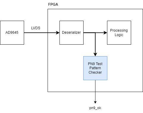
To bring up a board like the one shown below, with an AD9645 outputting samples over an LVDS link and an FPGA receiving them, I like to have the test pattern checker(s) built directly into the FPGA. In this article, I’ll show you how to implement such a test pattern checker using the LFSR components generated by the web-based airhdl code generator. We’ll be looking at the PN9 checker, but once you understand how it’s done, you’ll find it very easy to design your own checker for PN23 or other sequences.
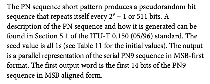
First let’s look at the AD9645 datasheet to find out how to PN9 sequence (also called the PN sequence short) is defined:
The description above is only part of the information we need to fully define the PN9 sequence. The missing part is the generator polynomial, which is given in another part of the datasheet as X^9 +X^5 +1. This is very mathematical way of describing a 9-bit shift-register with XOR feedback taps at bit positions 9 and 5 (using 1-based bit indexing).
The datasheet also gives the first words of the PN9 and PN23 sequences, which is super valuable information because it will allow us to easily check that we’re indeed generating the correct sequence:
To create a PN9 checker, we’ll be generating the expected PN9 sequence internally in the FPGA and checking that the words we receive from the FPGA actually match the expected ones. Of course, we’ll need to somehow synchronize the internally-generated sequence with the received one. For that, we’ll just wait until the initial value shown in the table above (0x1FE0) is received and then we’ll let our internal sequence generator update on every received word.
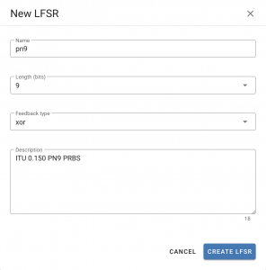
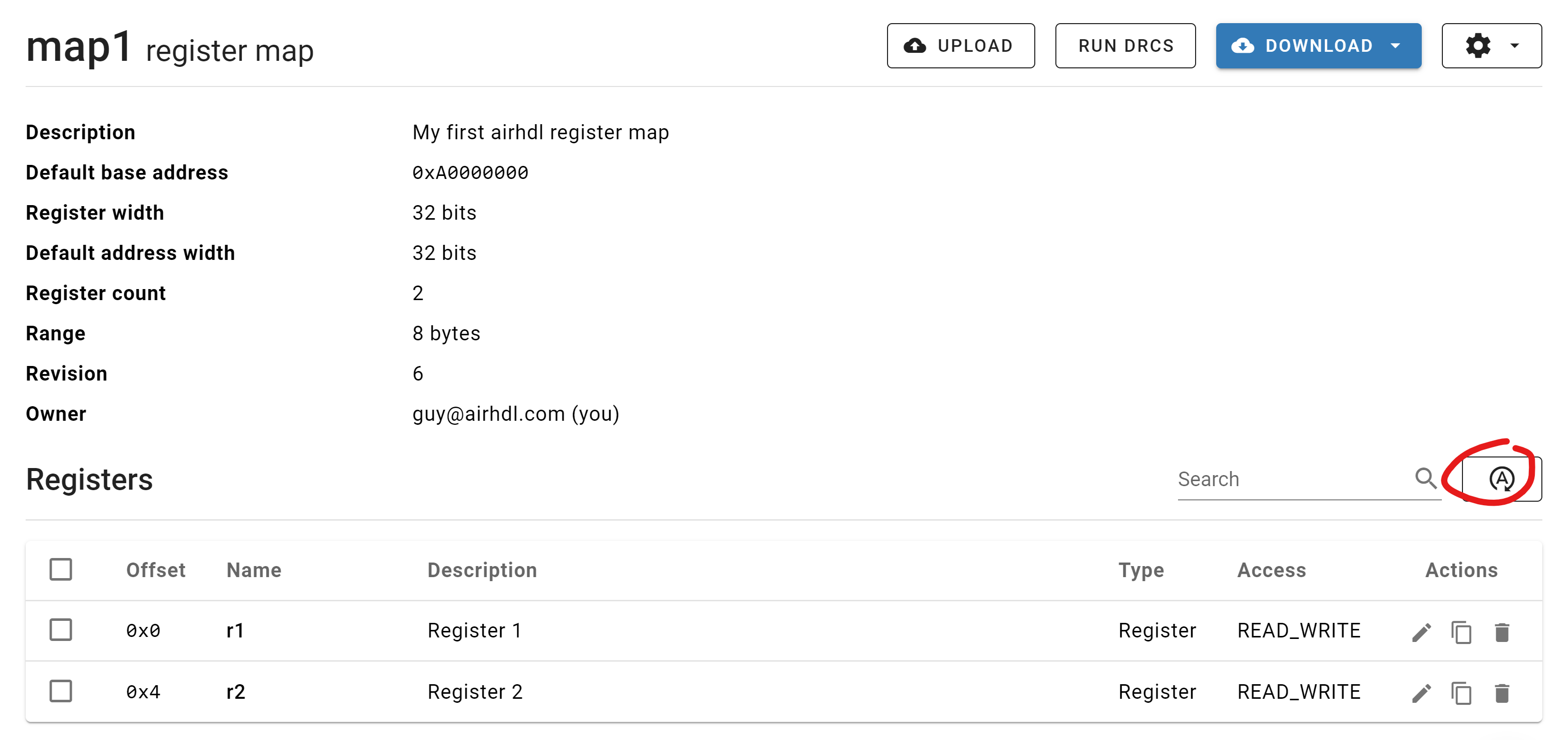
The first step is to head over to airhdl.com. After you have logged in, select the LFSRs entry in the left sidebar to show the Linear-Feedback Shift Registers view, and click the round “+” action button to bring up the New LFSR dialog:
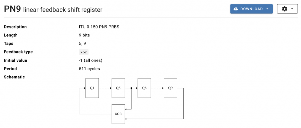
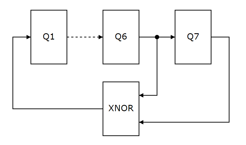
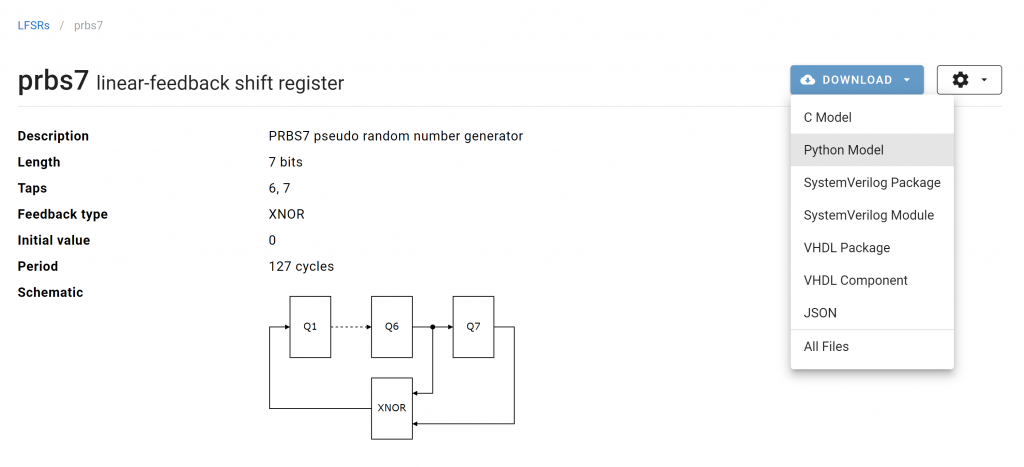
By setting the length to 9 bits and the feedback type to xor, airhdl will generate the following LFSR circuit. Note that based on the configured length of the LFSR (9 bits), airhdl automatically computes the correct positions of the feedback taps (5 and 9):
If you’re curious about the sequence of numbers that the circuit shown above generates, you can download the corresponding Python model and run it like this:
% python PN9_lfsr.py
1FF
1FE
1FC
1F8
1F0
1E0
1C1
183
107
00F
01E
03D
07B
0F7
1EF
1DF
The output above shows the first 16 states of this 9-bit LFSR (as we have said above, the sequence repeats every 2^9 – 1 = 511 cycles). This is not exactly the sequence that the AD9645 will output when placed in the PN9 test mode though, as the AD9645 is a 14-bit ADC and the PN9 circuit has a 9-bit word length. The AD9645 datasheet explains how to construct the 14-bit words from the LFSR output:
Using the airhdl-generated Python model for our PN9 LFSR, let’s look at the first 14 output words in binary form (we can use the -r bin option for that):
% python PN9_lfsr.py -r bin 14
111111111
111111110
111111100
111111000
111110000
111100000
111000001
110000011
100000111
000001111
000011110
000111101
001111011
011110111
As explained above, we can construct the first 14-bit word of the PN9 sequence by concatenating the MSBs of the LFSR’s first 14 output words: 11_1111_1110_0000. In order to match the two’s complement sequence that is indicated in the datasheet, we also need to invert the MSB, which gives us 01_1111_1110_0000 = 0x1FE0. This nicely matches the initial value of the PN sequence short from the table above!
Of course, there is always the risk that this is pure coincidence and a bit of paranoia is always a good thing for a developer; so let’s compute one more output word. This time we’ll ask our Python model to output the first 28 LFSR output words, and take the MSBs of the last 14 words:
% python PN9_lfsr.py -r bin 28
(...)
111101111
111011111
110111110
101111100
011111000
111110001
111100010
111000101
110001011
100010111
000101110
001011100
010111001
101110011
The corresponding output word, again obtained by concatenating the MSBs of the 9-bit LFSR states equals 11_1101_1111_0001. Inverting the MSB and converting the word to hexadecimal gives 0x1DF1, which matches the second output sample of the PN sequence short in the table above. At this point, the result being a pure coincidence is quite unlikely and we’ll assume that our algorithm works fine.
We now have a clear understanding of the algorithm for generating the 14-bit PN9 sequence. The next step is to design the corresponding checker circuit, using a hardware description language such as VHDL. As a starting point, we can download the VHDL package for our pn9 LFSR from the airhdl.com website. This package contains all the constants and a function we need to get us started:
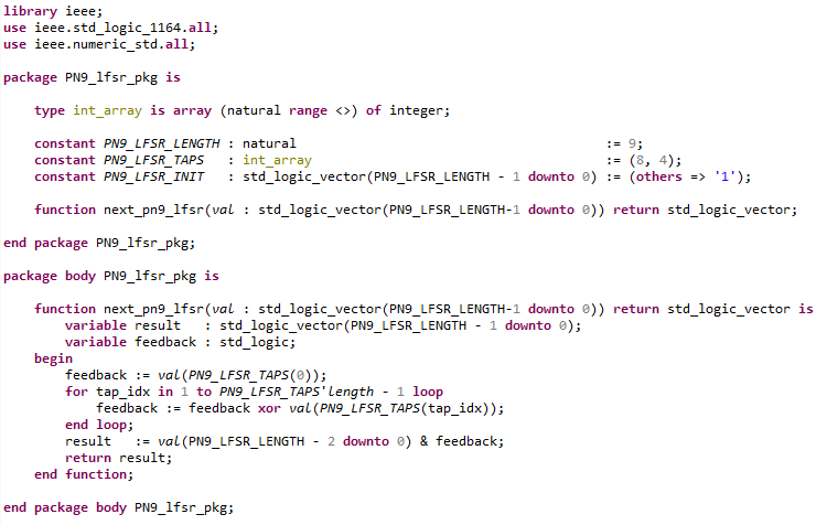
In particular, the next_pn9_lfsr function allows us to compute the next LFSR state, given the current one.
The principle of operation for our checker is as follows:
- Receive the first 14-bit ADC output word, let’s call it
adc_output[n]. - Using the
next_pn9_lfsrfunction, compute the next expected ADC output word; let’s call itadc_expected[n+1]. - Wait for the next ADC output word,
adc_output[n+1], and compare it toadc_expected[n+1]. If both values match, declare the test pattern checker synchronized and proceed with step 2. If there is a mismatch, the pattern checker is not synchronized and re-start at step 1.
The checker has two states: SYNC and TRACK. In the SYNC state, the checker waits until the PN9 initial value, which is given in the datasheet as 0x1FE0, appears on the data input. When that happens, the checker jumps into the TRACK state where it checks that every subsequent input word matches the next expected word from the PN9 sequence. As long as this is the case, the checker is considered synchronized and this is reflected by the pn9_ok output port being asserted high. If at any time an input word doesn’t match the next expected word, the checker immediately de-asserts its pn9_ok and jumps back into the SYNC state.
When doing hardware tests, you can connect the pn9_ok signal to a debug port of your FPGA design for easy monitoring using an oscilloscope. That way you can just trigger on falling edges of the pn9_ok signal to catch any bit errors, even transient ones.
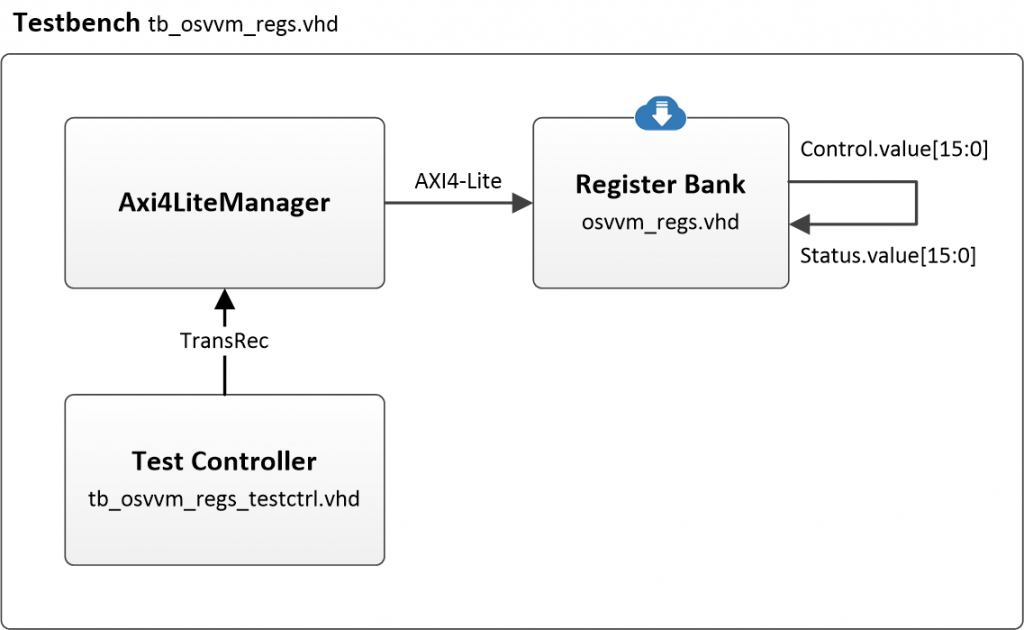
The VHDL code for the PN9 checker, including a VUnit testbench, is available on the airhdl GitHub. We hope you’ll find this useful!
