How to use an airhdl Register Bank in a Xilinx Vivado Project
To use an airhdl-generated AXI4-Lite register bank in a Xilinx Vivado project, you can either add the register bank as a module in a block design, or instantiate it in the RTL code.
Option 1: add the Register Bank as a Module in a Xilinx Vivado Block Design
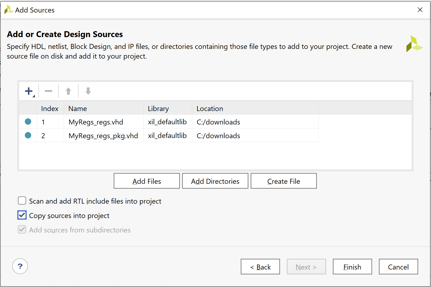
The easiest was to instantiate an airhdl register bank in a Xilinx Vivado project is to add it as a module to a block design. For that, the first step is to download both the component/module and the package files corresponding to your register map from the web application, or to generate them using the command line generator. Then, add both source files to your Vivado project using the Add Sources Flow Navigator entry, making sure to select the Add or create design sources flow:
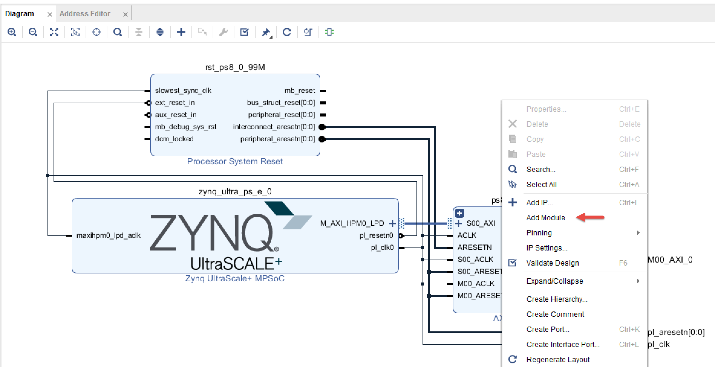
Then, open the block design for your project (e.g. by clicking Open Block Design in the Vivado Flow Navigator), right-click anywhere in the block diagram and select Add Module... in the context menu:
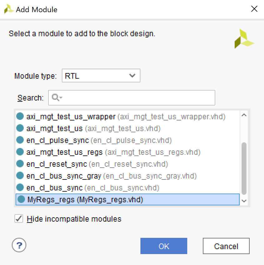
This brings up the the Add Module dialog, where you can select the register bank you have added to the project in the step before.
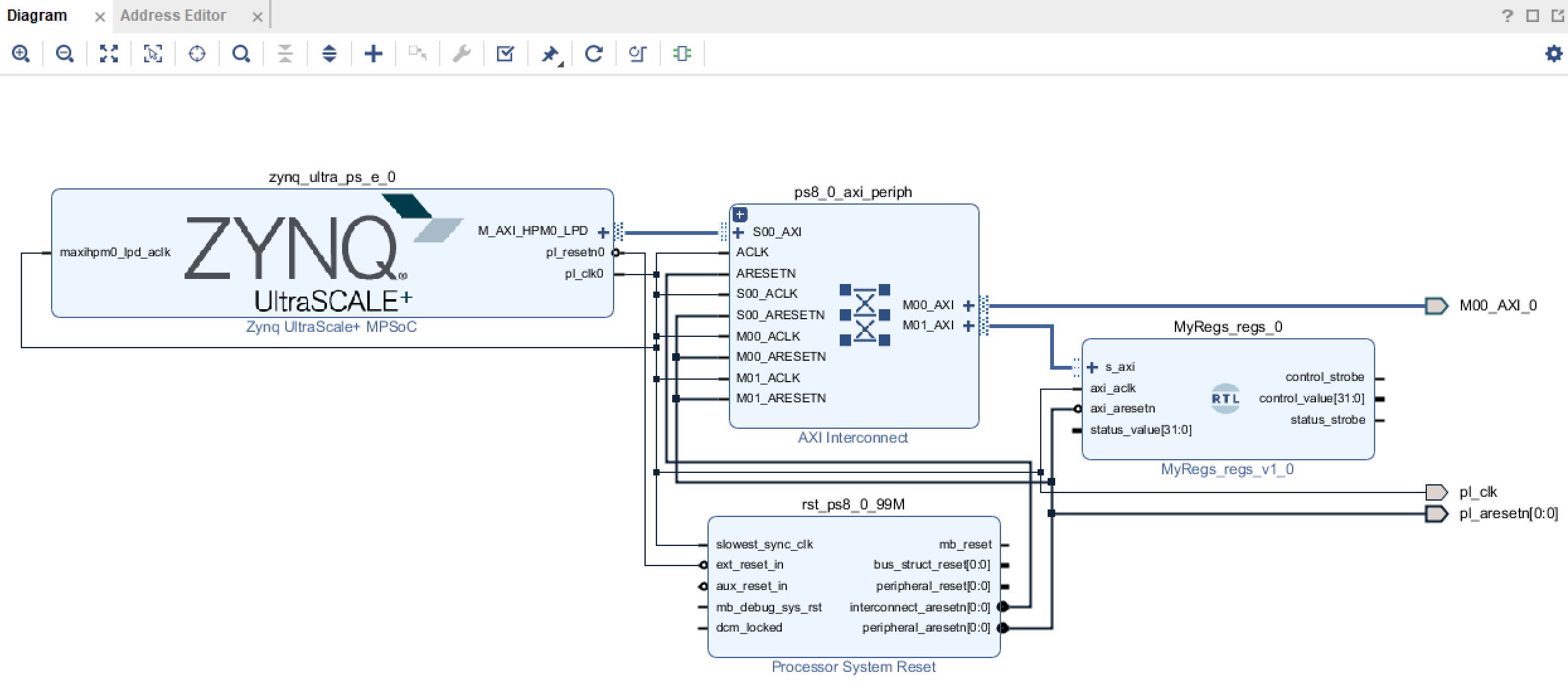
After adding the register bank component to the block diagram, you can use Connection Automation to connect the register bank's clock, reset and AXI4-Lite interface to the rest of the system.
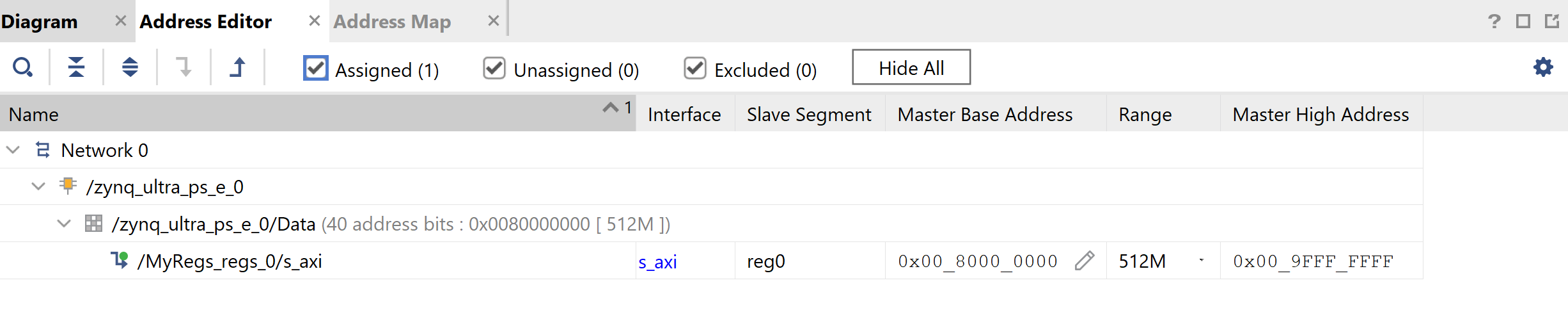
Finally, open the Address Editor tab of the block design and check that the register bank component has been assigned both a valid Master Base Address and a valid Range. In the example below, you can see that Vivado has set the register bank's base address to 0x8000_0000, and its range to 512M:
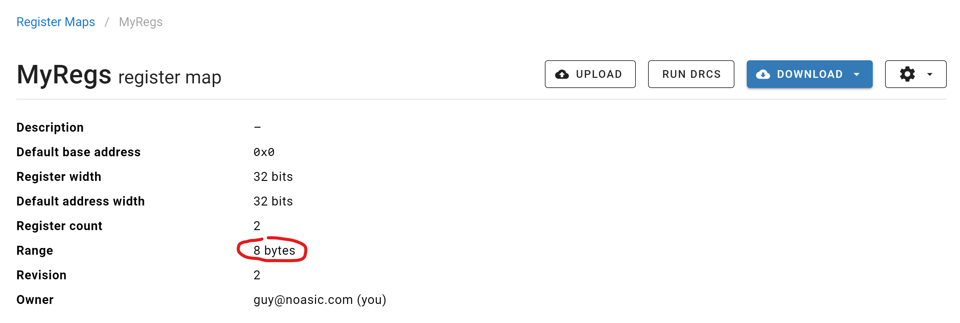
To find out the actual range of a register bank, open the corresponding Register Map view at airhdl.com and look for the Range information. In the example below, the range is 8 bytes:
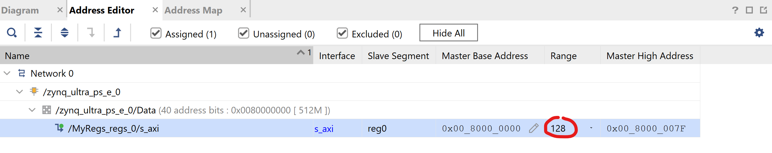
To avoid unnecessarily wasting address space, make sure to set the Range field in the Vivado Address Editor to the smallest value that is greater than or equal to the register map's actual range:
Finally, connect the register bank's user ports to your user logic, and run the Validate Design command to check that the design is correct.
Option 2: Instantiate the Register Component in the RTL Code
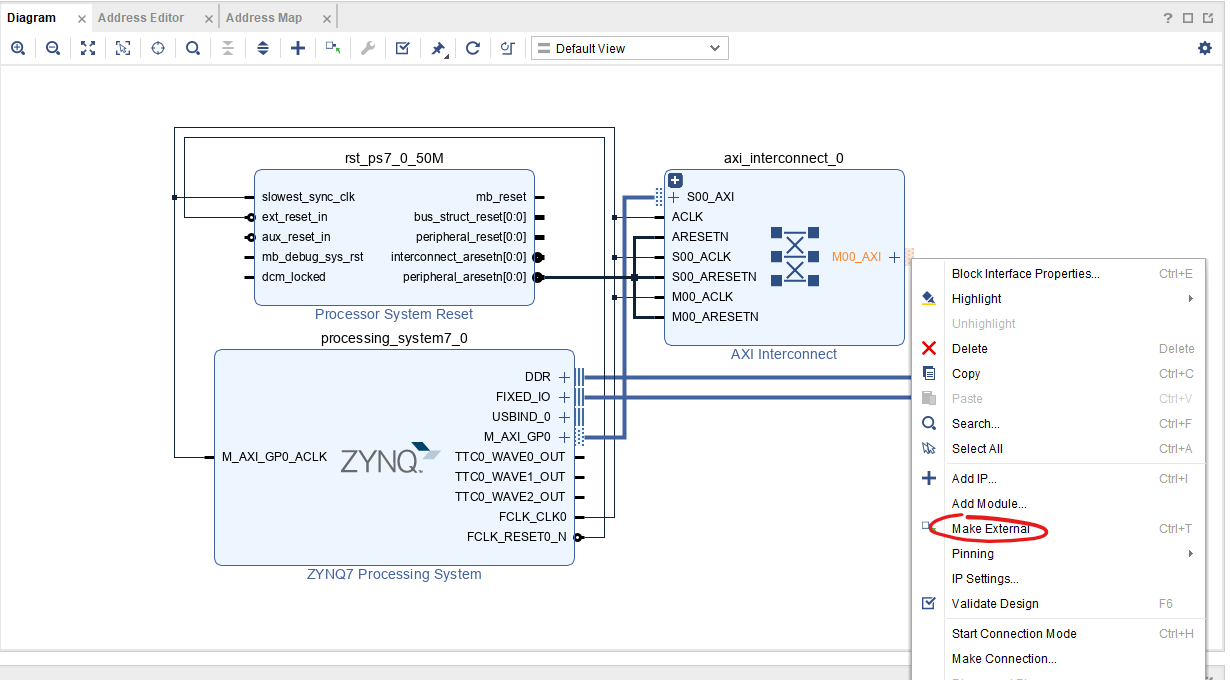
In case you cannot or do not want to add the register component as a module to a block design, you can instantiate it in the RTL code. For that, the first step is to create a new AXI4-Lite port in your block design. The easiest way to do that is to right-click an AXI Interconnect's master interface, and to select the Make External menu entry:
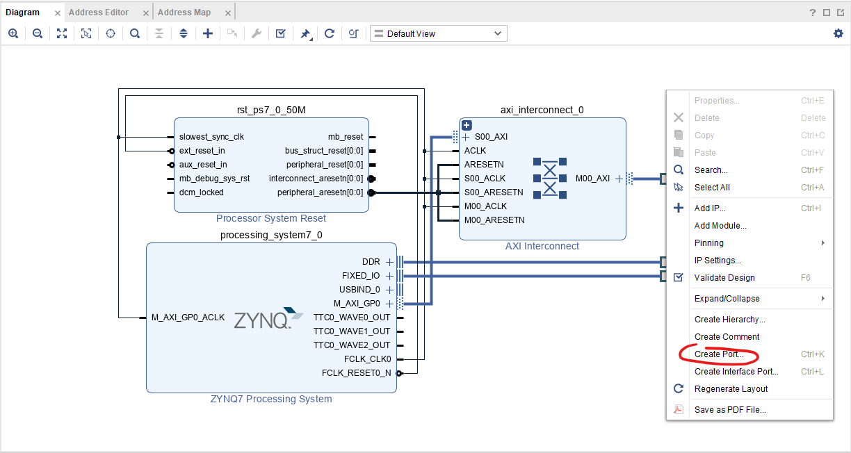
To provide AXI clock and reset signals for the register bank, add the corresponding ports by right-clicking anywhere in the block diagram and selecting Create Port... in the context menu:
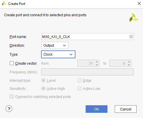
Create the clock port:
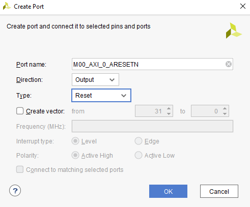
Create the reset port:
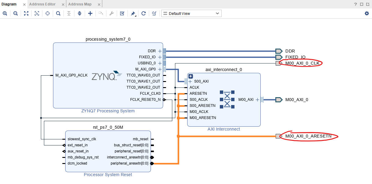
Connect the newly created clock and reset ports to the corresponding clock and reset nets:
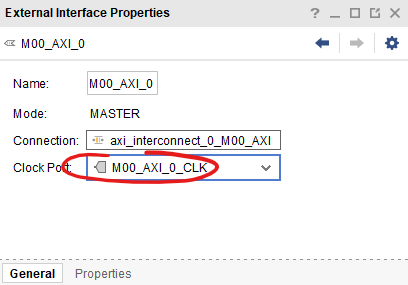
Next you need to associate the clock signal with the AXI4-Lite interface. For that, open the External Interface Properties view of the M00_AXI_0 port and set the corresponding clock port to the clock port you have created above:
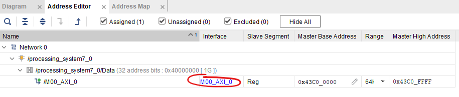
In the Address Editor tab, assign an address range to the AXI interface:
In the Block Diagram view, click on the Validate Design button to check your block diagram. Proceed only if the validation is successful.
In the Sources view, right-click on the block diagram and select Create HDL Wrapper...
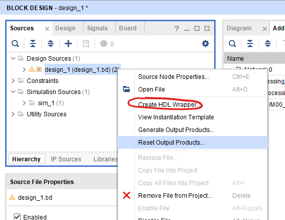
In the Create HDL Wrapper dialog, leave the options at their default values and click OK.
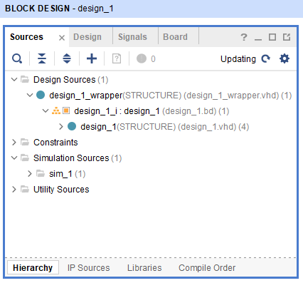
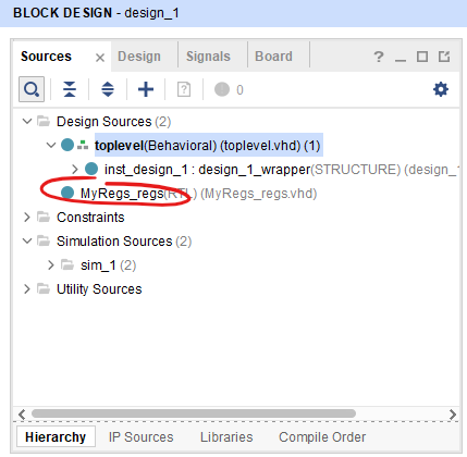
Your sources should now look like this:
Using Add Sources, create a toplevel VHDL file. Instantiate the block diagram wrapper in the toplevel file and connect all the non-AXI ports of the block diagram wrapper to toplevel ports:
library IEEE;
use IEEE.STD_LOGIC_1164.ALL;

entity toplevel is
port (
    DDR_addr : inout STD_LOGIC_VECTOR ( 14 downto 0 );
    DDR_ba : inout STD_LOGIC_VECTOR ( 2 downto 0 );
    DDR_cas_n : inout STD_LOGIC;
    DDR_ck_n : inout STD_LOGIC;
    DDR_ck_p : inout STD_LOGIC;
    DDR_cke : inout STD_LOGIC;
    DDR_cs_n : inout STD_LOGIC;
    DDR_dm : inout STD_LOGIC_VECTOR ( 3 downto 0 );
    DDR_dq : inout STD_LOGIC_VECTOR ( 31 downto 0 );
    DDR_dqs_n : inout STD_LOGIC_VECTOR ( 3 downto 0 );
    DDR_dqs_p : inout STD_LOGIC_VECTOR ( 3 downto 0 );
    DDR_odt : inout STD_LOGIC;
    DDR_ras_n : inout STD_LOGIC;
    DDR_reset_n : inout STD_LOGIC;
    DDR_we_n : inout STD_LOGIC;
    FIXED_IO_ddr_vrn : inout STD_LOGIC;
    FIXED_IO_ddr_vrp : inout STD_LOGIC;
    FIXED_IO_mio : inout STD_LOGIC_VECTOR ( 53 downto 0 );
    FIXED_IO_ps_clk : inout STD_LOGIC;
    FIXED_IO_ps_porb : inout STD_LOGIC;
    FIXED_IO_ps_srstb : inout STD_LOGIC
);
end toplevel;

architecture Behavioral of toplevel is

    signal M00_AXI_0_ARESETN : STD_LOGIC_VECTOR ( 0 to 0 );
    signal M00_AXI_0_CLK : STD_LOGIC;
    signal M00_AXI_0_araddr : STD_LOGIC_VECTOR ( 31 downto 0 );
    signal M00_AXI_0_arburst : STD_LOGIC_VECTOR ( 1 downto 0 );
    signal M00_AXI_0_arcache : STD_LOGIC_VECTOR ( 3 downto 0 );
    signal M00_AXI_0_arid : STD_LOGIC_VECTOR ( 11 downto 0 );
    signal M00_AXI_0_arlen : STD_LOGIC_VECTOR ( 3 downto 0 );
    signal M00_AXI_0_arlock : STD_LOGIC_VECTOR ( 1 downto 0 );
    signal M00_AXI_0_arprot : STD_LOGIC_VECTOR ( 2 downto 0 );
    signal M00_AXI_0_arqos : STD_LOGIC_VECTOR ( 3 downto 0 );
    signal M00_AXI_0_arready : STD_LOGIC;
    signal M00_AXI_0_arsize : STD_LOGIC_VECTOR ( 2 downto 0 );
    signal M00_AXI_0_arvalid : STD_LOGIC;
    signal M00_AXI_0_awaddr : STD_LOGIC_VECTOR ( 31 downto 0 );
    signal M00_AXI_0_awburst : STD_LOGIC_VECTOR ( 1 downto 0 );
    signal M00_AXI_0_awcache : STD_LOGIC_VECTOR ( 3 downto 0 );
    signal M00_AXI_0_awid : STD_LOGIC_VECTOR ( 11 downto 0 );
    signal M00_AXI_0_awlen : STD_LOGIC_VECTOR ( 3 downto 0 );
    signal M00_AXI_0_awlock : STD_LOGIC_VECTOR ( 1 downto 0 );
    signal M00_AXI_0_awprot : STD_LOGIC_VECTOR ( 2 downto 0 );
    signal M00_AXI_0_awqos : STD_LOGIC_VECTOR ( 3 downto 0 );
    signal M00_AXI_0_awready : STD_LOGIC;
    signal M00_AXI_0_awsize : STD_LOGIC_VECTOR ( 2 downto 0 );
    signal M00_AXI_0_awvalid : STD_LOGIC;
    signal M00_AXI_0_bid : STD_LOGIC_VECTOR ( 11 downto 0 );
    signal M00_AXI_0_bready : STD_LOGIC;
    signal M00_AXI_0_bresp : STD_LOGIC_VECTOR ( 1 downto 0 );
    signal M00_AXI_0_bvalid : STD_LOGIC;
    signal M00_AXI_0_rdata : STD_LOGIC_VECTOR ( 31 downto 0 );
    signal M00_AXI_0_rid : STD_LOGIC_VECTOR ( 11 downto 0 );
    signal M00_AXI_0_rlast : STD_LOGIC;
    signal M00_AXI_0_rready : STD_LOGIC;
    signal M00_AXI_0_rresp : STD_LOGIC_VECTOR ( 1 downto 0 );
    signal M00_AXI_0_rvalid : STD_LOGIC;
    signal M00_AXI_0_wdata : STD_LOGIC_VECTOR ( 31 downto 0 );
    signal M00_AXI_0_wid : STD_LOGIC_VECTOR ( 11 downto 0 );
    signal M00_AXI_0_wlast : STD_LOGIC;
    signal M00_AXI_0_wready : STD_LOGIC;
    signal M00_AXI_0_wstrb : STD_LOGIC_VECTOR ( 3 downto 0 );
    signal M00_AXI_0_wvalid : STD_LOGIC;

begin

    inst_design_1 : entity work.design_1_wrapper
    port map (
        M00_AXI_0_CLK => M00_AXI_0_CLK,
        M00_AXI_0_ARESETN => M00_AXI_0_ARESETN,
        DDR_cas_n => DDR_cas_n,
        DDR_cke => DDR_cke,
        DDR_ck_n => DDR_ck_n,
        DDR_ck_p => DDR_ck_p,
        DDR_cs_n => DDR_cs_n,
        DDR_reset_n => DDR_reset_n,
        DDR_odt => DDR_odt,
        DDR_ras_n => DDR_ras_n,
        DDR_we_n => DDR_we_n,
        DDR_ba => DDR_ba,
        DDR_addr => DDR_addr,
        DDR_dm => DDR_dm,
        DDR_dq => DDR_dq,
        DDR_dqs_n => DDR_dqs_n,
        DDR_dqs_p => DDR_dqs_p,
        FIXED_IO_mio => FIXED_IO_mio,
        FIXED_IO_ddr_vrn => FIXED_IO_ddr_vrn,
        FIXED_IO_ddr_vrp => FIXED_IO_ddr_vrp,
        FIXED_IO_ps_srstb => FIXED_IO_ps_srstb,
        FIXED_IO_ps_clk => FIXED_IO_ps_clk,
        FIXED_IO_ps_porb => FIXED_IO_ps_porb,
        M00_AXI_0_arvalid => M00_AXI_0_arvalid,
        M00_AXI_0_awvalid => M00_AXI_0_awvalid,
        M00_AXI_0_bready => M00_AXI_0_bready,
        M00_AXI_0_rready => M00_AXI_0_rready,
        M00_AXI_0_wlast => M00_AXI_0_wlast,
        M00_AXI_0_wvalid => M00_AXI_0_wvalid,
        M00_AXI_0_arid => M00_AXI_0_arid,
        M00_AXI_0_awid => M00_AXI_0_awid,
        M00_AXI_0_wid => M00_AXI_0_wid,
        M00_AXI_0_arburst => M00_AXI_0_arburst,
        M00_AXI_0_arlock => M00_AXI_0_arlock,
        M00_AXI_0_arsize => M00_AXI_0_arsize,
        M00_AXI_0_awburst => M00_AXI_0_awburst,
        M00_AXI_0_awlock => M00_AXI_0_awlock,
        M00_AXI_0_awsize => M00_AXI_0_awsize,
        M00_AXI_0_arprot => M00_AXI_0_arprot,
        M00_AXI_0_awprot => M00_AXI_0_awprot,
        M00_AXI_0_araddr => M00_AXI_0_araddr,
        M00_AXI_0_awaddr => M00_AXI_0_awaddr,
        M00_AXI_0_wdata => M00_AXI_0_wdata,
        M00_AXI_0_arcache => M00_AXI_0_arcache,
        M00_AXI_0_arlen => M00_AXI_0_arlen,
        M00_AXI_0_arqos => M00_AXI_0_arqos,
        M00_AXI_0_awcache => M00_AXI_0_awcache,
        M00_AXI_0_awlen => M00_AXI_0_awlen,
        M00_AXI_0_awqos => M00_AXI_0_awqos,
        M00_AXI_0_wstrb => M00_AXI_0_wstrb,
        M00_AXI_0_arready => M00_AXI_0_arready,
        M00_AXI_0_awready => M00_AXI_0_awready,
        M00_AXI_0_bvalid => M00_AXI_0_bvalid,
        M00_AXI_0_rlast => M00_AXI_0_rlast,
        M00_AXI_0_rvalid => M00_AXI_0_rvalid,
        M00_AXI_0_wready => M00_AXI_0_wready,
        M00_AXI_0_bid => M00_AXI_0_bid,
        M00_AXI_0_rid => M00_AXI_0_rid,
        M00_AXI_0_bresp => M00_AXI_0_bresp,
        M00_AXI_0_rresp => M00_AXI_0_rresp,
        M00_AXI_0_rdata => M00_AXI_0_rdata
    );

end Behavioral;
Download your register map's VHDL Package and Component files (e.g. MyRegs_regs.vhd and MyRegs_pkg.vhd) from airhdl.com and add them to your project:
Instantiate the register component inside your toplevel file, connecting the AXI ports to the block diagram wrapper's AXI ports, and the user ports to your user logic:
library IEEE;
use IEEE.STD_LOGIC_1164.ALL;

entity toplevel is
port (
    DDR_addr : inout STD_LOGIC_VECTOR ( 14 downto 0 );
    DDR_ba : inout STD_LOGIC_VECTOR ( 2 downto 0 );
    DDR_cas_n : inout STD_LOGIC;
    DDR_ck_n : inout STD_LOGIC;
    DDR_ck_p : inout STD_LOGIC;
    DDR_cke : inout STD_LOGIC;
    DDR_cs_n : inout STD_LOGIC;
    DDR_dm : inout STD_LOGIC_VECTOR ( 3 downto 0 );
    DDR_dq : inout STD_LOGIC_VECTOR ( 31 downto 0 );
    DDR_dqs_n : inout STD_LOGIC_VECTOR ( 3 downto 0 );
    DDR_dqs_p : inout STD_LOGIC_VECTOR ( 3 downto 0 );
    DDR_odt : inout STD_LOGIC;
    DDR_ras_n : inout STD_LOGIC;
    DDR_reset_n : inout STD_LOGIC;
    DDR_we_n : inout STD_LOGIC;
    FIXED_IO_ddr_vrn : inout STD_LOGIC;
    FIXED_IO_ddr_vrp : inout STD_LOGIC;
    FIXED_IO_mio : inout STD_LOGIC_VECTOR ( 53 downto 0 );
    FIXED_IO_ps_clk : inout STD_LOGIC;
    FIXED_IO_ps_porb : inout STD_LOGIC;
    FIXED_IO_ps_srstb : inout STD_LOGIC
);
end toplevel;

architecture Behavioral of toplevel is

    signal M00_AXI_0_ARESETN : STD_LOGIC_VECTOR ( 0 to 0 );
    signal M00_AXI_0_CLK : STD_LOGIC;
    signal M00_AXI_0_araddr : STD_LOGIC_VECTOR ( 31 downto 0 );
    signal M00_AXI_0_arburst : STD_LOGIC_VECTOR ( 1 downto 0 );
    signal M00_AXI_0_arcache : STD_LOGIC_VECTOR ( 3 downto 0 );
    signal M00_AXI_0_arid : STD_LOGIC_VECTOR ( 11 downto 0 );
    signal M00_AXI_0_arlen : STD_LOGIC_VECTOR ( 3 downto 0 );
    signal M00_AXI_0_arlock : STD_LOGIC_VECTOR ( 1 downto 0 );
    signal M00_AXI_0_arprot : STD_LOGIC_VECTOR ( 2 downto 0 );
    signal M00_AXI_0_arqos : STD_LOGIC_VECTOR ( 3 downto 0 );
    signal M00_AXI_0_arready : STD_LOGIC;
    signal M00_AXI_0_arsize : STD_LOGIC_VECTOR ( 2 downto 0 );
    signal M00_AXI_0_arvalid : STD_LOGIC;
    signal M00_AXI_0_awaddr : STD_LOGIC_VECTOR ( 31 downto 0 );
    signal M00_AXI_0_awburst : STD_LOGIC_VECTOR ( 1 downto 0 );
    signal M00_AXI_0_awcache : STD_LOGIC_VECTOR ( 3 downto 0 );
    signal M00_AXI_0_awid : STD_LOGIC_VECTOR ( 11 downto 0 );
    signal M00_AXI_0_awlen : STD_LOGIC_VECTOR ( 3 downto 0 );
    signal M00_AXI_0_awlock : STD_LOGIC_VECTOR ( 1 downto 0 );
    signal M00_AXI_0_awprot : STD_LOGIC_VECTOR ( 2 downto 0 );
    signal M00_AXI_0_awqos : STD_LOGIC_VECTOR ( 3 downto 0 );
    signal M00_AXI_0_awready : STD_LOGIC;
    signal M00_AXI_0_awsize : STD_LOGIC_VECTOR ( 2 downto 0 );
    signal M00_AXI_0_awvalid : STD_LOGIC;
    signal M00_AXI_0_bid : STD_LOGIC_VECTOR ( 11 downto 0 );
    signal M00_AXI_0_bready : STD_LOGIC;
    signal M00_AXI_0_bresp : STD_LOGIC_VECTOR ( 1 downto 0 );
    signal M00_AXI_0_bvalid : STD_LOGIC;
    signal M00_AXI_0_rdata : STD_LOGIC_VECTOR ( 31 downto 0 );
    signal M00_AXI_0_rid : STD_LOGIC_VECTOR ( 11 downto 0 );
    signal M00_AXI_0_rlast : STD_LOGIC;
    signal M00_AXI_0_rready : STD_LOGIC;
    signal M00_AXI_0_rresp : STD_LOGIC_VECTOR ( 1 downto 0 );
    signal M00_AXI_0_rvalid : STD_LOGIC;
    signal M00_AXI_0_wdata : STD_LOGIC_VECTOR ( 31 downto 0 );
    signal M00_AXI_0_wid : STD_LOGIC_VECTOR ( 11 downto 0 );
    signal M00_AXI_0_wlast : STD_LOGIC;
    signal M00_AXI_0_wready : STD_LOGIC;
    signal M00_AXI_0_wstrb : STD_LOGIC_VECTOR ( 3 downto 0 );
    signal M00_AXI_0_wvalid : STD_LOGIC;

    -- User signals:
    signal control_value : std_logic_vector(31 downto 0);
    signal status_value : std_logic_vector(31 downto 0);

begin

    inst_design_1 : entity work.design_1_wrapper
    port map (
        M00_AXI_0_CLK => M00_AXI_0_CLK,
        M00_AXI_0_ARESETN => M00_AXI_0_ARESETN,
        DDR_cas_n => DDR_cas_n,
        DDR_cke => DDR_cke,
        DDR_ck_n => DDR_ck_n,
        DDR_ck_p => DDR_ck_p,
        DDR_cs_n => DDR_cs_n,
        DDR_reset_n => DDR_reset_n,
        DDR_odt => DDR_odt,
        DDR_ras_n => DDR_ras_n,
        DDR_we_n => DDR_we_n,
        DDR_ba => DDR_ba,
        DDR_addr => DDR_addr,
        DDR_dm => DDR_dm,
        DDR_dq => DDR_dq,
        DDR_dqs_n => DDR_dqs_n,
        DDR_dqs_p => DDR_dqs_p,
        FIXED_IO_mio => FIXED_IO_mio,
        FIXED_IO_ddr_vrn => FIXED_IO_ddr_vrn,
        FIXED_IO_ddr_vrp => FIXED_IO_ddr_vrp,
        FIXED_IO_ps_srstb => FIXED_IO_ps_srstb,
        FIXED_IO_ps_clk => FIXED_IO_ps_clk,
        FIXED_IO_ps_porb => FIXED_IO_ps_porb,
        M00_AXI_0_arvalid => M00_AXI_0_arvalid,
        M00_AXI_0_awvalid => M00_AXI_0_awvalid,
        M00_AXI_0_bready => M00_AXI_0_bready,
        M00_AXI_0_rready => M00_AXI_0_rready,
        M00_AXI_0_wlast => M00_AXI_0_wlast,
        M00_AXI_0_wvalid => M00_AXI_0_wvalid,
        M00_AXI_0_arid => M00_AXI_0_arid,
        M00_AXI_0_awid => M00_AXI_0_awid,
        M00_AXI_0_wid => M00_AXI_0_wid,
        M00_AXI_0_arburst => M00_AXI_0_arburst,
        M00_AXI_0_arlock => M00_AXI_0_arlock,
        M00_AXI_0_arsize => M00_AXI_0_arsize,
        M00_AXI_0_awburst => M00_AXI_0_awburst,
        M00_AXI_0_awlock => M00_AXI_0_awlock,
        M00_AXI_0_awsize => M00_AXI_0_awsize,
        M00_AXI_0_arprot => M00_AXI_0_arprot,
        M00_AXI_0_awprot => M00_AXI_0_awprot,
        M00_AXI_0_araddr => M00_AXI_0_araddr,
        M00_AXI_0_awaddr => M00_AXI_0_awaddr,
        M00_AXI_0_wdata => M00_AXI_0_wdata,
        M00_AXI_0_arcache => M00_AXI_0_arcache,
        M00_AXI_0_arlen => M00_AXI_0_arlen,
        M00_AXI_0_arqos => M00_AXI_0_arqos,
        M00_AXI_0_awcache => M00_AXI_0_awcache,
        M00_AXI_0_awlen => M00_AXI_0_awlen,
        M00_AXI_0_awqos => M00_AXI_0_awqos,
        M00_AXI_0_wstrb => M00_AXI_0_wstrb,
        M00_AXI_0_arready => M00_AXI_0_arready,
        M00_AXI_0_awready => M00_AXI_0_awready,
        M00_AXI_0_bvalid => M00_AXI_0_bvalid,
        M00_AXI_0_rlast => M00_AXI_0_rlast,
        M00_AXI_0_rvalid => M00_AXI_0_rvalid,
        M00_AXI_0_wready => M00_AXI_0_wready,
        M00_AXI_0_bid => M00_AXI_0_bid,
        M00_AXI_0_rid => M00_AXI_0_rid,
        M00_AXI_0_bresp => M00_AXI_0_bresp,
        M00_AXI_0_rresp => M00_AXI_0_rresp,
        M00_AXI_0_rdata => M00_AXI_0_rdata
    );

    myregs_inst : entity work.MyRegs_regs
    port map(
        -- Clock and Reset
        axi_aclk    => M00_AXI_0_CLK,
        axi_aresetn => M00_AXI_0_ARESETN,
        -- AXI Write Address Channel
        s_axi_awaddr  => M00_AXI_0_awaddr,
        s_axi_awprot  => M00_AXI_0_awprot,
        s_axi_awvalid => M00_AXI_0_awvalid,
        s_axi_awready => M00_AXI_0_awready,
        -- AXI Write Data Channel
        s_axi_wdata   => M00_AXI_0_wdata,
        s_axi_wstrb   => M00_AXI_0_wstrb,
        s_axi_wvalid  => M00_AXI_0_wvalid,
        s_axi_wready  => M00_AXI_0_wready,
        -- AXI Read Address Channel
        s_axi_araddr  => M00_AXI_0_araddr,
        s_axi_arprot  => M00_AXI_0_arprot,
        s_axi_arvalid => M00_AXI_0_arvalid,
        s_axi_arready => M00_AXI_0_arready,
        -- AXI Read Data Channel
        s_axi_rdata   => M00_AXI_0_rdata,
        s_axi_rresp   => M00_AXI_0_rresp,
        s_axi_rvalid  => M00_AXI_0_rvalid,
        s_axi_rready  => M00_AXI_0_rready,
        -- AXI Write Response Channel
        s_axi_bresp   => M00_AXI_0_bresp,
        s_axi_bvalid  => M00_AXI_0_bvalid,
        s_axi_bready  => M00_AXI_0_bready,
        -- User Ports
        control_strobe => open,
        control_value => control_value,
        status_strobe => open,
        status_value => status_value
    );

    -- User logic
    status_value <= control_value;

end Behavioral;
Finally, synthesize and implement the design.