Register Map Elements
Register maps contain a list of register map elements, which can be registers, arrays of registers or memory interfaces.
Access Modes
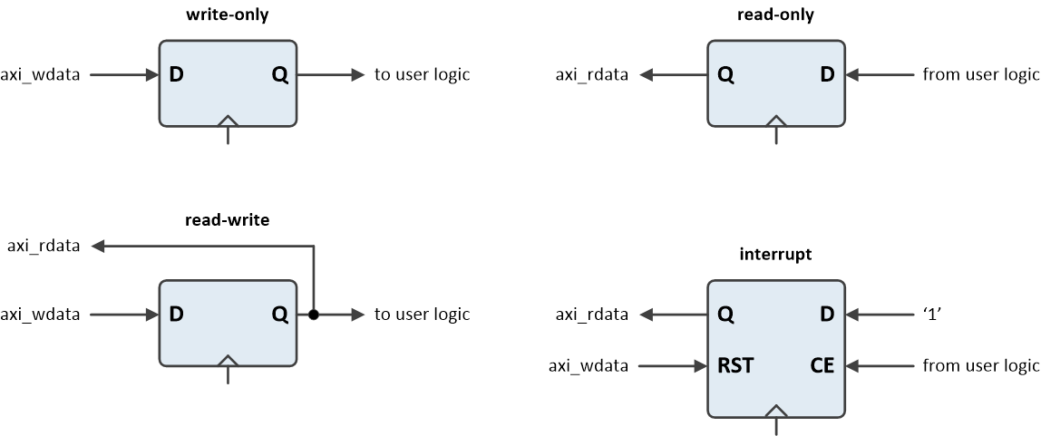
Access modes define how register map elements interface with the bus and the user logic. In airhdl, there are four different access modes:
- Write-only elements are written from the bus, and read from the user logic. Write-only elements can be used for control registers that you don't need to read back from the bus. For large register banks, replacing some of the read-write registers with write-only registers can be useful to relax the timing on the read data path.
- Read-write elements can be both written and read from the bus. The register value is driven to the user logic.
- Read-only elements can only be read from the bus. The register value is driven from the user logic.
- Interrupt elements are set from the user logic. Their value can be read from the bus. Interrupt element bits are cleared from the bus by writing '1' to the corresponding bits, a process also known as "write-one-to-clear".
Trying to read from a write-only register, or write to a read-only register will result in an AXI4 SLVERR error response.
Registers
Registers are the simplest type of register map element. They translate into flip-flops in the generated register bank, and each register occupies 4 bytes in the address space.
Depending on the register's access mode, airhdl generates different ports in the RTL component.
For write-only and read-write registers, airhdl generates the following ports:
| Name | Direction | Description |
|---|---|---|
<register name>_strobe | output | a strobe signal that is pulsed every time the register is written from the bus |
<register name>_<field_name> | output | the current value of the corresponding register field (one port per field) |
For read-write registers with volatile fields, an additional input port is generated:
| Name | Direction | Description |
|---|---|---|
<register name>_<field_name>_rd | input | the read value of a volatile field (one port per field) |
For read-only registers, airhdl generates the following ports:
| Name | Direction | Description |
|---|---|---|
<register name>_strobe | output | a strobe signal that is pulsed every time the register is read from the bus |
<register name>_<field_name> | output | the current value of the corresponding register field (one port per field) |
For interrupt registers, airhdl generates the following ports:
| Name | Direction | Description |
|---|---|---|
<register name>_<field_name>_set | input | the set signal, which allows the user logic to set the corresponding register field (one port per field) |
Register Arrays
Registers arrays are two-dimensional registers of configurable length. They can be used to store data such as filter coefficients that require parallel access to all elements.
Depending on the register's access mode, airhdl generates different ports in the RTL component.
For write-only and read-write registers:
| Name | Direction | Description |
|---|---|---|
<register name>_strobe [0:N-1] | output | a strobe signal that is pulsed every time the register is written from the bus |
<register_name>_<field_name> [0:N-1] | output | the current value of the corresponding register field (one port per field) |
For read-only registers:
| Name | Direction | Description |
|---|---|---|
<register name>_strobe [0:N-1] | output | a strobe signal that is pulsed every time the register is written from the bus |
<register_name>_<field_name> [0:N-1] | input | the current value of the corresponding regsiter field (one port per field) |
For interrupt registers:
| Name | Direction | Description |
|---|---|---|
<register name>_<field_name>_set [0:N-1] | input | the set signal, which allows the user logic to set the corresponding register field (one port per field). |
Memories
Memories are actually memory interfaces, which can be used to connect synchronous RAMs like the Block RAMs found in Xilinx™ FPGAs to the generated register bank.
Depending on the access mode, the memory can then be written and/or read from the bus. Memories can be useful for implementing objects like look-up tables, which don't need parallel access to all elements at once in the user logic.
Memories have a configurable read latency of 1 to 5 clock cycles.
Unlike other register map elements, memories do not support the interrupt access mode.
Memory Ports
Depending on the memory's access mode, airhdl generates different ports in the RTL component.
For write-only memories:
| Name | Direction | Description |
|---|---|---|
<memory name>_addr | output | the memory address word |
<memory name>_wen | output | the memory write-enable signal |
<memory name>_wdata | output | the memory write data word |
For read-write memories:
| Name | Direction | Description |
|---|---|---|
<memory name>_addr | output | the memory address word |
<memory name>_wen | output | the memory write-enable signal |
<memory name>_wdata | output | the memory write data word |
<memory name>_ren | output | the memory read-enable signal |
<memory name>_rdata | input | the memory read data word |
For read-only memories:
| Name | Direction | Description |
|---|---|---|
<memory name>_addr | output | the memory address word |
<memory name>_ren | output | the memory read-enable signal |
<memory name>_rdata | input | the memory read data word |
Memory Access Timings
Memory Write Timing
Memory writes are performed by asserting the *_wen
signals while outputting the write address on the *_addr
port and the write data on the *_wdata port.

Memory Read Timing
Memory reads assume a synchronous RAM with a read latency between 1 and
5 clock cycles. The following diagram illustrates a read access to a
memory with read latency of one clock cycle. The *_ren
signal can be used as an enable signal for the RAM cell.

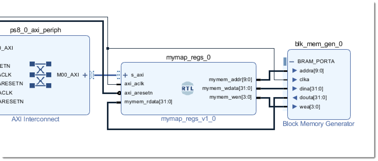
Connecting an External Memory to a Register Bank
The following schematic shows how to connect a Xilinx™ Block Memory IP
(blk_mem_gen_0) to the memory interface of an airhdl
generated register bank (mymap_regs_0) in the Xilinx™
Vivado™ block diagram editor.